SEM stands for a scanning electron microscope. Electron microscopes use electrons for imaging, in a similar way that light microscopes use visible light. SEMs use a specific set of coils to scan the beam in a raster-like pattern and use the electrons that are reflected or knocked off the near-surface region of a sample to form an image. Since the wavelength of electrons is much smaller than the wavelength of light, the resolution of SEMs is superior to that of a light microscope. Scanning Electron Microscopy technology has achieved a very powerful and versatile tool for performing characterization of materials. Over the past few years, it has achieved huge fame due to the rapidly shrinking of the dimension of materials that are used in several applications.
SEM or Scanning Electron Microscopes uses the electrons for imaging, in a way that is similar to that of light microscopes using visible light. A specific set of coils are used by SEM for scanning the beam in a raster-like pattern and use the electrons which are reflected or knocked off the near-surface region of a sample for forming an image. As the wavelength of electrons is much smaller than the wavelength of light, SEM's resolution is superior to that of a light microscope. In this type of microscope, the electron beam at first scans the sample by following a raster pattern. But at the beginning, the electrons are generated at the top of the column by the source electron. When their thermal energy overcomes the work function of the source material, these are emitted. After that, they are accelerated and attracted by the positively charged anode. The total electron column requires it to remain under vacuum. Like every other component of an electron microscope, the source of the electron is sealed inside a special chamber for preserving vacuum and protecting it from getting contaminated, vibrations and noise. The vacuum although it protects the electron source from getting contaminated, but also allows the user to acquire a high-resolution image. As the vacuum is absent, the other atoms and molecules can be present in the column. Their interaction with the electrons causes the electron beam for deflecting and reducing the image quality. Afterward, a heavy vacuum increases the collection efficiency of electrons by the detectors which are in the column. Researchers can get help with optimizing their material characterization process and save valuable time.
Are you trying to find a way to optimize your research processes and applications? Do you want to conduct better analyses in less time? Choose the right microscope for your research from Dutco Tennant LLC.
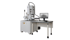
JSM-7900F Schottky Field Emission Scanning Electron Microscope (FESEM)